A good PCB layout for the ACPL-217-500E involves keeping the input and output circuits separate, using a ground plane, and minimizing the length of the signal traces. It's also recommended to use a 4-layer PCB with a dedicated power plane and a dedicated ground plane.
To ensure reliability in high-temperature applications, it's essential to follow proper thermal management practices, such as providing adequate heat sinking, using a thermally conductive material for the PCB, and ensuring good airflow around the device.
The ACPL-217-500E has built-in ESD protection, but it's still recommended to follow proper ESD handling procedures during assembly and testing. This includes using an ESD wrist strap, ESD mat, and ESD-protected packaging.
The ACPL-217-500E is rated for up to 500V, but it's essential to ensure that the device is used within its specified voltage ratings and that proper isolation is maintained between the input and output circuits.
To troubleshoot common issues with the ACPL-217-500E, start by checking the PCB layout and ensuring that the input and output circuits are properly isolated. Also, verify that the device is operated within its specified voltage and current ratings. If issues persist, consult the datasheet and application notes for guidance.
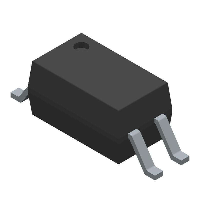 ACPL-217-500E datasheet
by Avago Technologies
ACPL-217-500E datasheet
by Avago Technologies