A 4-layer PCB with a solid ground plane and a separate power plane is recommended. The device should be placed near the edge of the board to minimize signal reflections. A 50-ohm microstrip transmission line should be used for the RF signal path.
The device requires a single 3.3V power supply. A 10uF capacitor should be placed between the VCC pin and ground to filter out noise. A 1kohm resistor should be used to bias the VBIAS pin to 1.5V.
The device is rated for operation from -40°C to 85°C. However, optimal performance is achieved between 0°C to 70°C.
Use a spectrum analyzer to verify the RF signal frequency and amplitude. Check the DC power supply voltage and current consumption. Use a logic analyzer to verify the digital control signals. Consult the datasheet and application notes for specific troubleshooting guidelines.
Yes, but impedance matching networks may be required to ensure optimal performance. Consult the datasheet and application notes for guidance on impedance matching.
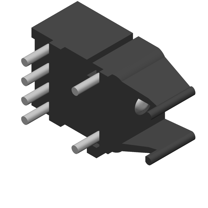 AFBR-2624Z datasheet
by Avago Technologies
AFBR-2624Z datasheet
by Avago Technologies
 Findchips
 Findchips