A thermal pad is recommended under the package to improve heat dissipation. A minimum of 2oz copper thickness and a thermal relief pattern are suggested. Refer to the application note AN-111 for more details.
The AO3415A requires a stable input voltage (VIN) and a proper biasing circuit to ensure optimal performance. A recommended biasing circuit is shown in the datasheet, figure 12. Ensure the input voltage is within the recommended range (4.5V to 28V) and the biasing resistors are chosen correctly.
The AO3415A is an ESD-sensitive device. Handle the device by the body, avoid touching the pins, and use an anti-static wrist strap or mat. Store the device in an anti-static bag or tube to prevent damage.
Start by verifying the input voltage, biasing circuit, and PCB layout. Check for overheating, incorrect pin connections, or incorrect component values. Refer to the datasheet and application notes for troubleshooting guidelines.
The AO3415A is built with high-quality materials and manufacturing processes to ensure reliability. It meets industry standards for automotive and industrial applications, including AEC-Q100 and IATF 16949 certifications.
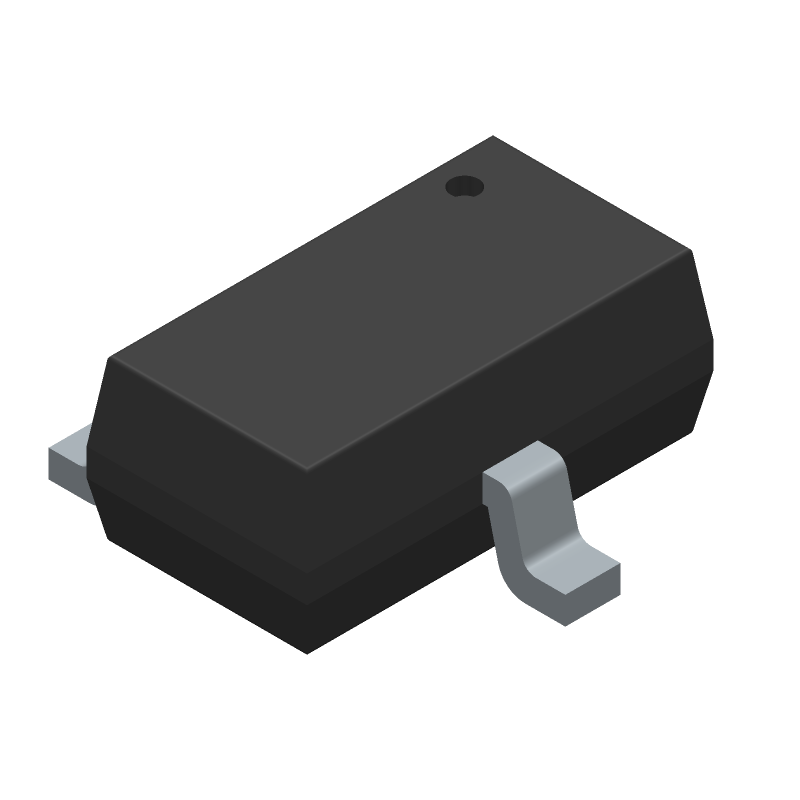 AO3415A datasheet
by Alpha & Omega Semiconductor
AO3415A datasheet
by Alpha & Omega Semiconductor
 Findchips
 Findchips