A recommended PCB layout for optimal thermal performance would be to have a solid ground plane on the bottom layer, and to use thermal vias to connect the exposed pad to the ground plane. This helps to dissipate heat efficiently.
To ensure proper power-on and power-off, it is recommended to follow a soft-start sequence, where the input voltage is ramped up slowly to prevent inrush currents. Additionally, a power-good signal can be used to monitor the output voltage and ensure it is within the specified range.
To prevent damage, it is recommended to handle the device by the body, avoiding touching the pins or electrical connections. Additionally, anti-static precautions should be taken, such as using an anti-static wrist strap or mat, to prevent electrostatic discharge damage.
To troubleshoot issues, it is recommended to first check the input voltage and current, as well as the output voltage and current. Then, check the PCB layout and component placement to ensure they meet the recommended layout guidelines. If issues persist, consult the datasheet and application notes for further guidance.
The device has a maximum junction temperature of 150°C. To ensure reliable operation over temperature, it is recommended to keep the device within the specified operating temperature range, and to ensure good thermal conductivity between the device and the PCB. A thermal analysis can be performed to determine the device's thermal performance in the specific application.
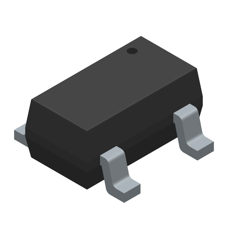 AP22802AW5-7 datasheet
by Diodes Incorporated
AP22802AW5-7 datasheet
by Diodes Incorporated