The recommended PCB footprint for the B350B-13-F is a standard SOT23 package with a 1.3mm x 1.3mm body size. A minimum pad size of 0.8mm x 0.8mm is recommended for reliable soldering.
To ensure proper biasing, connect the input pin (VIN) to a stable voltage source, and the output pin (VOUT) to a load or a voltage regulator. Ensure the input voltage is within the recommended operating range (2.5V to 5.5V) and the output current does not exceed the maximum rating (150mA).
The B350B-13-F has an operating temperature range of -40°C to 125°C. However, it's recommended to operate the device within a temperature range of -20°C to 85°C for optimal performance and reliability.
While the B350B-13-F is a general-purpose voltage regulator, it may not meet the specific requirements for high-reliability or automotive applications. For such applications, consider using a device specifically designed for those markets, such as the AEC-Q100 qualified B350B-13-F-A or equivalent.
To calculate the power dissipation of the B350B-13-F, use the formula: Pd = (VIN - VOUT) x IOUT. Where Pd is the power dissipation, VIN is the input voltage, VOUT is the output voltage, and IOUT is the output current. Ensure the calculated power dissipation does not exceed the maximum rating (0.5W).
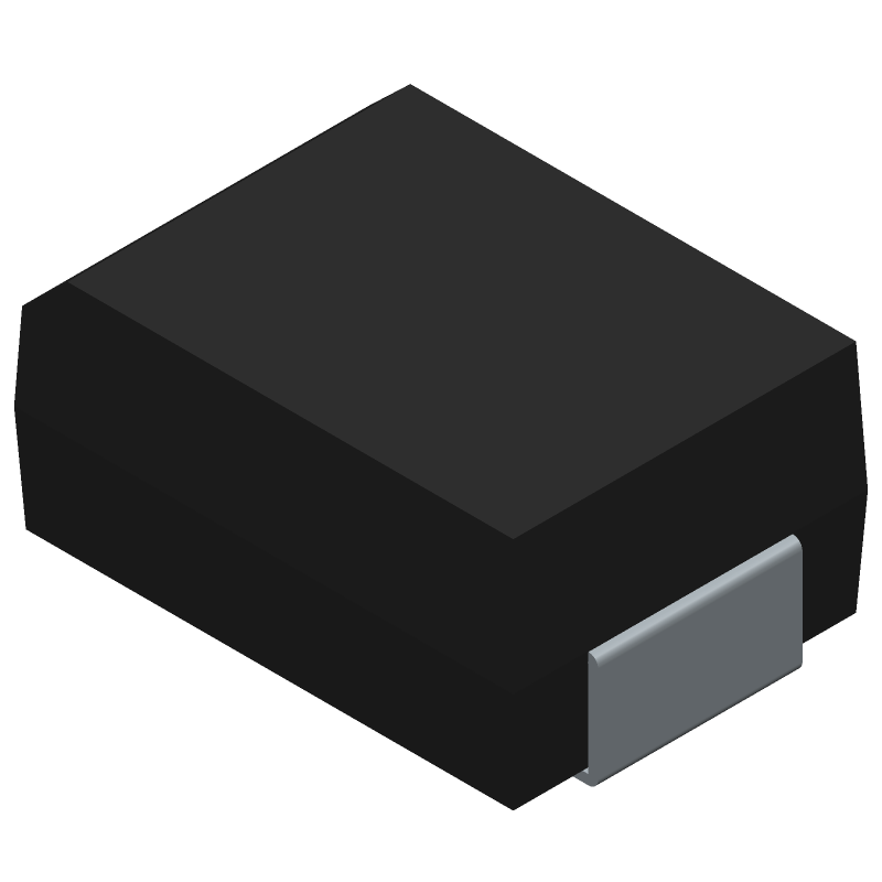 B350B-13-F datasheet
by Diodes Incorporated
B350B-13-F datasheet
by Diodes Incorporated