A 2-layer or 4-layer PCB with a thermal pad connected to a large copper area on the bottom layer is recommended. This helps to dissipate heat efficiently and reduce thermal resistance.
Implement a robust thermal management system, including a heat sink, thermal interface material, and a cooling fan if necessary. Also, ensure that the device is operated within the recommended temperature range and that the junction temperature is monitored and controlled.
Monitor the device's junction temperature, voltage, and current during reliability testing. Also, track the device's performance parameters, such as switching frequency, rise and fall times, and output voltage ripple.
Implement proper handling and storage procedures, such as using anti-static bags and wrist straps. Also, design the PCB with EOS and ESD protection in mind, including the use of TVS diodes and resistors to limit voltage and current surges.
Use a soldering temperature of 250°C to 260°C, with a soldering time of 3 to 5 seconds. Ensure that the soldering iron is clean and well-tinned to prevent oxidation and ensure good wetting.
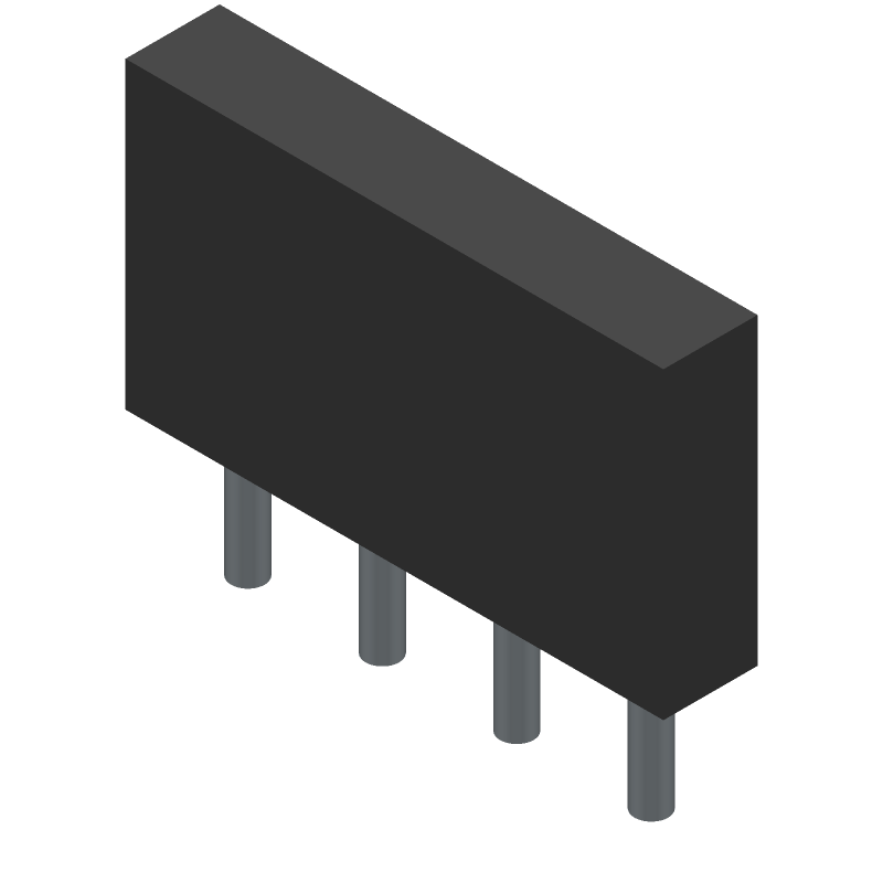 D2SB80 datasheet
by Taiwan Semiconductor
D2SB80 datasheet
by Taiwan Semiconductor
 Findchips
 Findchips