A good PCB layout for the DMG2307L-7 should include a solid ground plane, wide power traces, and a thermal relief pattern under the device to facilitate heat dissipation. A minimum of 2oz copper thickness is recommended.
To ensure proper biasing, connect the gate to a voltage source through a resistor (e.g., 1kΩ) and add a pull-down resistor (e.g., 10kΩ) from the gate to ground. This helps maintain a stable gate-source voltage and prevents unwanted turn-on.
Monitor the device's junction temperature (TJ), drain-source voltage (VDS), and drain current (ID) to prevent overheating. Ensure TJ remains below the maximum rating (150°C) and VDS and ID are within the recommended operating ranges.
Yes, the DMG2307L-7 is suitable for high-frequency switching applications up to 1 MHz. However, ensure proper PCB layout, decoupling, and snubber circuits to minimize ringing and electromagnetic interference (EMI).
Handle the device with ESD-protective equipment, and ensure the PCB has ESD protection circuits, such as TVS diodes or ESD-protection arrays, to prevent damage from static electricity.
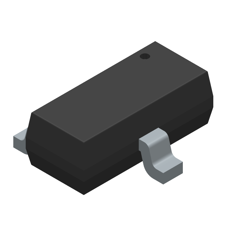 DMG2307L-7 datasheet
by Diodes Incorporated
DMG2307L-7 datasheet
by Diodes Incorporated