A good PCB layout for the DRC3143Z0L involves keeping the input and output traces short and separate, using a solid ground plane, and placing decoupling capacitors close to the device. A 4-layer PCB with a dedicated power plane and a solid ground plane is recommended.
To ensure reliability in high-temperature applications, it's essential to follow proper thermal design and management practices. This includes providing adequate heat sinking, using thermal interface materials, and ensuring good airflow around the device. Additionally, derating the device's power consumption and operating frequency can help reduce thermal stress.
The DRC3143Z0L has built-in ESD protection, but it's still important to follow proper ESD handling and storage procedures to prevent damage. This includes using ESD-safe materials, grounding oneself before handling the device, and storing the device in ESD-safe packaging.
While the DRC3143Z0L is designed to operate in a variety of environments, high humidity can still affect its performance and reliability. To mitigate this, it's recommended to use conformal coating, potting, or other environmental protection methods to prevent moisture ingress.
The recommended soldering conditions for the DRC3143Z0L include a peak temperature of 260°C, a soldering time of 3 seconds or less, and a soldering iron temperature of 350°C or less. It's also important to use a solder with a melting point below 220°C to prevent damage to the device.
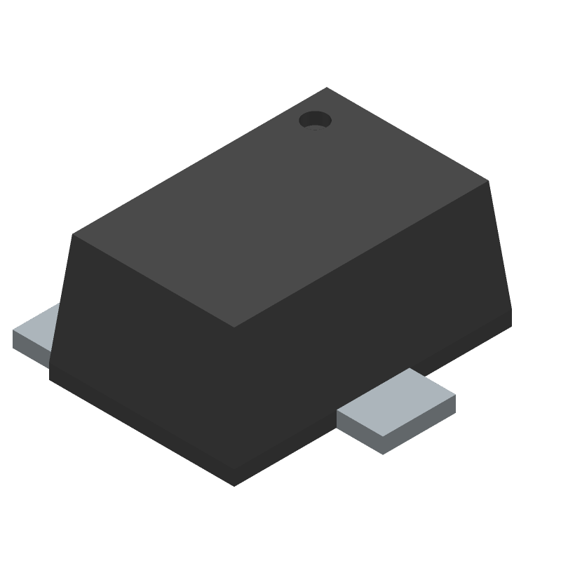 DRC3143Z0L datasheet
by Panasonic Electronic Components
DRC3143Z0L datasheet
by Panasonic Electronic Components
 Findchips
