The recommended PCB layout for the DS1249Y-70IND# involves keeping the device away from high-current carrying traces, using a solid ground plane, and minimizing the length of the traces connected to the VCC and GND pins. Additionally, it's recommended to use a 0.1uF decoupling capacitor between VCC and GND, and to keep the input and output traces separate to minimize noise coupling.
To ensure proper power-up and initialization of the DS1249Y-70IND#, it's recommended to follow a power-up sequence where VCC is applied before the input signals, and to hold the input signals in a valid state until the device is fully powered up. Additionally, the device requires a minimum of 100ms to power up and initialize, so it's recommended to add a delay or a power-on reset circuit to ensure the device is fully operational before applying input signals.
The DS1249Y-70IND# is rated for operation over the industrial temperature range of -40°C to +85°C. However, it's recommended to derate the device's performance and reliability at temperatures above +70°C, and to ensure proper thermal management to prevent overheating.
The DS1249Y-70IND# has built-in ESD protection, but it's still recommended to follow proper ESD handling procedures during assembly and testing. This includes using ESD-safe materials, grounding oneself before handling the device, and using ESD protection devices such as TVS diodes or ESD suppressors on the input and output lines.
The recommended input signal range for the DS1249Y-70IND# is between 0V and VCC, with a maximum input voltage of 5.5V. It's recommended to ensure the input signals are within this range to prevent damage to the device or incorrect operation.
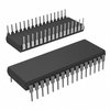 DS1249Y-70IND# datasheet
by Maxim Integrated Products
DS1249Y-70IND# datasheet
by Maxim Integrated Products