A good PCB layout for the DSC300100L involves keeping the input and output traces separate, using a solid ground plane, and minimizing the length of the input traces to reduce noise and parasitic inductance.
To ensure proper biasing, connect the input pins to a voltage source through a resistor, and connect the output pins to a load resistor. The recommended bias voltage is typically 1/2 of the supply voltage.
The maximum power dissipation of the DSC300100L is typically around 1W. To prevent overheating, ensure good airflow around the device, use a heat sink if necessary, and keep the ambient temperature below 85°C.
To prevent ESD damage, handle the DSC300100L in an ESD-protected environment, use an anti-static wrist strap or mat, and avoid touching the device's pins or leads.
Store the DSC300100L in a dry, cool place (below 30°C and 60% RH) away from direct sunlight and moisture. Avoid exposing the device to extreme temperatures, humidity, or physical stress.
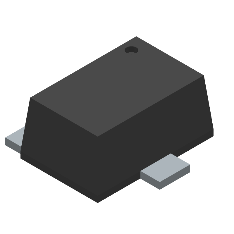 DSC300100L datasheet
by Panasonic Electronic Components
DSC300100L datasheet
by Panasonic Electronic Components