A good PCB layout for optimal thermal performance would be to have a solid ground plane on the bottom layer, and a thermal relief pattern on the top layer. This helps to dissipate heat efficiently. Additionally, it's recommended to have a minimum of 2oz copper thickness and a thermal via array under the device to improve heat dissipation.
To ensure proper biasing, it's essential to follow the recommended voltage and current ratings specified in the datasheet. The device should be biased in a way that the voltage across the device is within the recommended range, and the current is within the maximum rated current. A stable voltage source and a low-ESR capacitor are also recommended to ensure optimal performance.
To prevent damage, it's essential to handle the device by the body and not the leads. Avoid touching the leads or the die, as the oils from your skin can cause damage. Use an anti-static wrist strap or mat to prevent electrostatic discharge (ESD) damage. Also, avoid bending or flexing the leads, as this can cause mechanical stress and damage to the device.
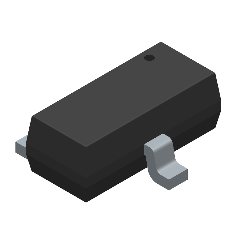
The correct package orientation for the FMMT619TA can be determined by referring to the datasheet or the manufacturer's documentation. The device has a distinct marking on the top side, which indicates the pin 1 location. The device should be oriented such that the marking is facing upwards and the pins are facing away from the user.
The FMMT619TA meets various reliability and quality standards, including AEC-Q101, which is a standard for automotive-grade semiconductor devices. The device also meets the requirements of IEC 60747-1 and IEC 60747-5 for semiconductor devices. Additionally, the device is manufactured in accordance with the ISO 9001 quality management system.
 FMMT619TA datasheet
by Diodes Incorporated
FMMT619TA datasheet
by Diodes Incorporated
 Findchips
 Findchips