A good PCB layout for the GBU801 involves keeping the input and output traces separate, using a ground plane, and placing the device close to the power source. Additionally, using a shielded inductor and keeping the switching node (pin 5) away from sensitive nodes can help reduce EMI.
The inductor value depends on the input voltage, output voltage, and switching frequency. A good starting point is to use the inductor value recommended in the datasheet (e.g., 10uH). Then, adjust the value based on the specific application requirements, such as output current and ripple voltage.
The maximum ambient temperature for the GBU801 is 85°C. However, the device can operate up to 125°C junction temperature. It's essential to ensure proper thermal management to prevent overheating and ensure reliable operation.
Yes, the GBU801 is suitable for high-reliability applications. It's built with a robust design, and Diodes Incorporated provides a high level of quality control and testing to ensure the device meets the required standards. However, it's essential to follow proper design and manufacturing guidelines to ensure the device operates within its specifications.
To troubleshoot issues with the GBU801, start by checking the input voltage, output voltage, and current. Verify that the device is properly soldered and that the PCB layout is correct. Check for signs of overheating, such as excessive temperature or burning smells. Use an oscilloscope to check the switching node and output voltage waveforms. Consult the datasheet and application notes for guidance on troubleshooting specific issues.
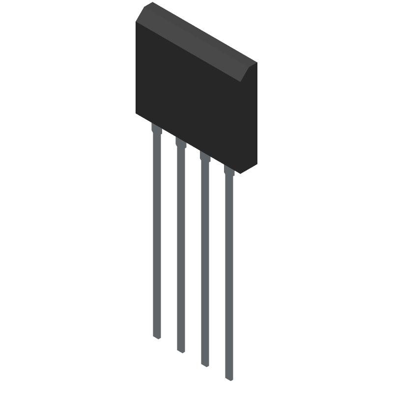 GBU801 datasheet
by Diodes Incorporated
GBU801 datasheet
by Diodes Incorporated