Broadcom recommends a 4-layer PCB with a solid ground plane, and thermal vias under the device to dissipate heat. A thermal pad on the bottom of the device should be connected to a thermal plane on the PCB.
Use a low-dropout regulator (LDO) with a high power supply rejection ratio (PSRR) to minimize noise and ripple. Ensure the power supply can provide the required current and voltage (1.8V, 3.3V, and 5V) with minimal voltage droop.
Pay attention to signal routing, impedance matching, and termination to minimize signal reflections and jitter. Use controlled impedance lines, and consider using differential signaling for high-speed signals.
Follow good EMC design practices, such as using shielding, filtering, and grounding techniques. Ensure the PCB layout and component placement minimize electromagnetic radiation and susceptibility.
Use a logic analyzer or oscilloscope to measure signal integrity and timing. For functional testing, use a test fixture or a development board with a suitable interface (e.g., JTAG, SPI, or I2C).
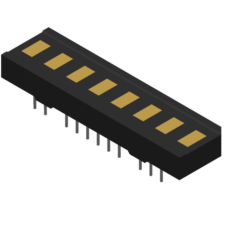 HCMS-3977 datasheet
by Avago Technologies
HCMS-3977 datasheet
by Avago Technologies