A good PCB layout for HCPL-0211-000E involves keeping the input and output traces separate, using a ground plane, and minimizing the length of the input traces. It's also recommended to use a 0.1uF capacitor between VCC and GND pins to filter out noise.
To ensure reliability in high-temperature applications, it's essential to follow the recommended operating temperature range of -40°C to 100°C. Additionally, consider using a heat sink or thermal pad to dissipate heat, and ensure good airflow around the device.
The maximum allowable voltage on the input pins of HCPL-0211-000E is 5.5V. Exceeding this voltage can cause damage to the device. It's recommended to use voltage limiting resistors or clamping diodes to protect the input pins.
Yes, HCPL-0211-000E can be used in high-frequency applications up to 10 Mbps. However, it's essential to follow proper PCB layout and termination techniques to minimize signal reflections and ensure signal integrity.
To troubleshoot issues with HCPL-0211-000E, start by verifying the input signal and power supply voltage. Check for proper PCB layout, termination, and decoupling. Use an oscilloscope to verify the input and output signals. If the issue persists, consult the datasheet and application notes or contact Broadcom Limited support.
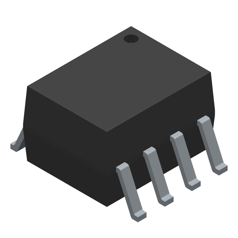 HCPL-0211-000E datasheet
by Avago Technologies
HCPL-0211-000E datasheet
by Avago Technologies