A good PCB layout for HCPL-0453-500E involves keeping the input and output circuits separate, using a ground plane, and minimizing track lengths and widths to reduce noise and electromagnetic interference (EMI).
To ensure reliable operation in high-temperature environments, ensure that the device is operated within its specified temperature range (-40°C to 100°C), and consider using a heat sink or thermal management system to prevent overheating.
Common failure modes of HCPL-0453-500E include overvoltage, overcurrent, and electrostatic discharge (ESD). To mitigate these, use voltage regulators, current limiters, and ESD protection circuits, and follow proper handling and storage procedures.
Yes, HCPL-0453-500E can be used in high-frequency applications, but its bandwidth is limited to 10 MHz. Above this frequency, the device's performance may degrade, and signal attenuation and distortion may occur.
To troubleshoot issues with HCPL-0453-500E, check the input voltage, output load, and PCB layout for any anomalies or non-compliance with the datasheet specifications. Use oscilloscopes and logic analyzers to debug the signal waveforms and timing.
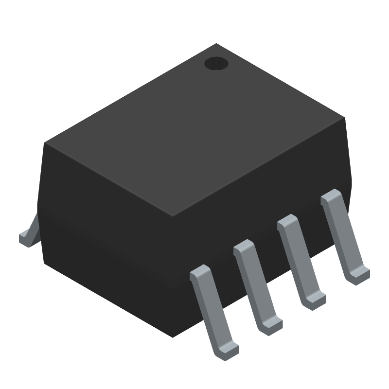 HCPL-0453-500E datasheet
by Avago Technologies
HCPL-0453-500E datasheet
by Avago Technologies
 Findchips
