A good PCB layout for HCPL-2212 involves keeping the input and output circuits separate, using a ground plane, and minimizing the length of the input and output traces. It's also recommended to use a shielded cable for the input signal and to keep the output circuitry away from the input circuitry.
To ensure reliability in high-temperature applications, it's essential to follow proper derating guidelines, ensure good thermal management, and consider using a heat sink if necessary. Additionally, selecting components with a high temperature rating and using a reliable soldering process can help ensure reliability.
Common failure modes of HCPL-2212 include input overvoltage, output short circuits, and excessive temperature. To mitigate these, ensure proper input voltage clamping, use a current-limiting resistor in the output circuit, and implement thermal monitoring and protection.
While HCPL-2212 is primarily designed for low-frequency applications, it can be used in high-frequency applications up to 25 kHz. However, it's essential to consider the device's bandwidth, slew rate, and propagation delay to ensure it meets the requirements of your specific application.
To ensure EMC when using HCPL-2212, follow proper PCB layout guidelines, use shielding and filtering techniques, and consider using a common-mode choke or ferrite bead to reduce electromagnetic interference (EMI).
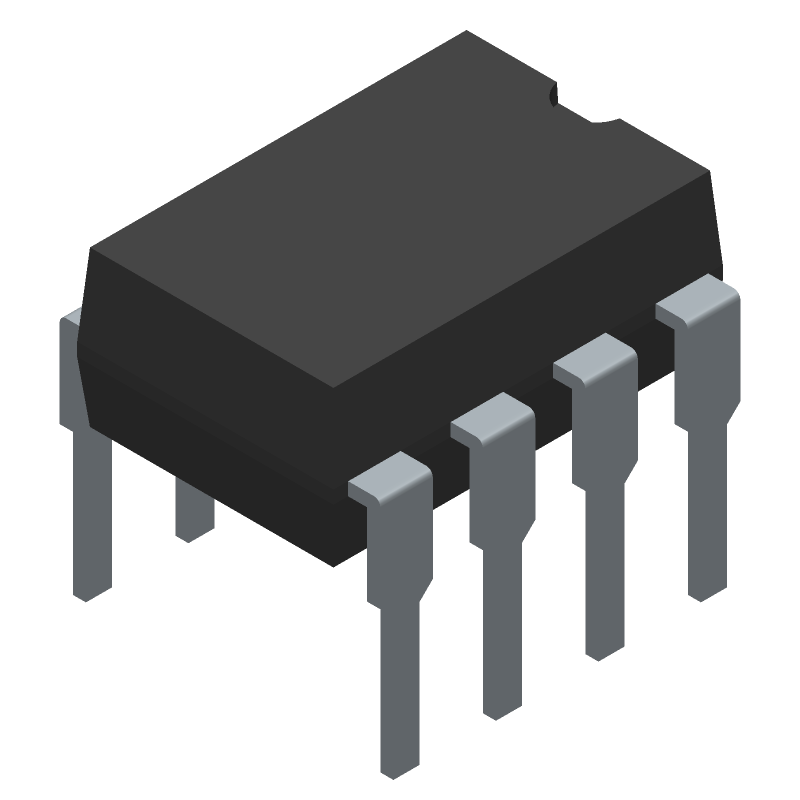 HCPL-2212 datasheet
by Avago Technologies
HCPL-2212 datasheet
by Avago Technologies
 Findchips
 Findchips