A good PCB layout for HCPL-3120 involves keeping the input and output circuits separate, using a ground plane, and minimizing the length of the input and output traces. It's also recommended to use a 0.1uF capacitor between VCC and GND pins to filter out noise.
To ensure reliability in high-temperature applications, it's essential to follow the recommended operating temperature range (−40°C to 100°C) and consider the derating of the device's current rating at higher temperatures. Additionally, ensure good thermal management, such as using a heat sink or thermal pad, to keep the junction temperature within the recommended range.
The maximum allowable voltage on the input pins of HCPL-3120 is 5.5V. Exceeding this voltage can cause damage to the device. It's recommended to use voltage limiting resistors or clamping diodes to protect the input pins from overvoltage conditions.
While HCPL-3120 is primarily designed for low-frequency applications, it can be used in high-frequency applications up to 25 kHz. However, the device's performance may degrade at higher frequencies due to internal capacitance and inductance. It's recommended to evaluate the device's performance in the specific application and consider using a faster optocoupler if necessary.
To troubleshoot issues with HCPL-3120, start by verifying the input signal and power supply voltage. Check for proper PCB layout, decoupling, and termination. Use an oscilloscope to measure the input and output waveforms, and verify that the device is operating within the recommended specifications. Consult the datasheet and application notes for guidance on troubleshooting specific issues.
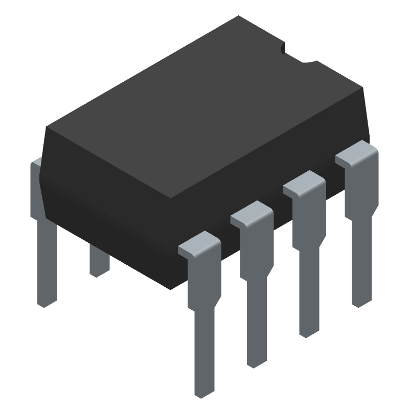 HCPL-3120 datasheet
by Avago Technologies
HCPL-3120 datasheet
by Avago Technologies
