A 4-layer PCB with a dedicated analog ground plane, proper decoupling, and short traces between the ADC and analog signal sources is recommended. Consult the Broadcom application note AN135 for more details.
Perform a full-scale calibration after power-up, and consider implementing a periodic calibration routine to compensate for temperature and voltage variations. Refer to the datasheet's calibration section for more information.
Use a low-jitter clock source (<100 ps) and ensure the clock signal is properly terminated and routed. A differential clock input is recommended to minimize noise and skew.
Use a reliable data transfer protocol (e.g., SPI or LVDS) and implement error detection and correction mechanisms, such as CRC or ECC, to ensure data integrity.
Ensure good airflow, use a heat sink or thermal pad if necessary, and follow the recommended PCB thermal design guidelines to keep the junction temperature below 125°C.
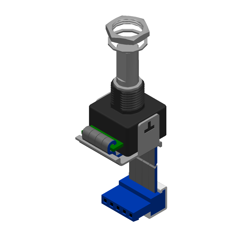 HRPG-AD32#16C datasheet
by Avago Technologies
HRPG-AD32#16C datasheet
by Avago Technologies