The recommended PCB layout for optimal thermal performance involves placing a thermal pad on the bottom of the package, using a 2-3 oz copper pour, and ensuring good airflow around the component.
To ensure reliable operation in high-temperature environments, it is recommended to derate the power dissipation according to the temperature derating curve provided in the datasheet, and to ensure good airflow around the component.
The maximum allowable voltage for the input pins is 5.5V, exceeding which may cause damage to the device.
Yes, the KBP301G-BP can be used in a switching power supply design, but it is recommended to ensure that the input voltage and frequency are within the specified limits, and to add proper filtering and protection circuits to prevent damage from voltage spikes and transients.
The power dissipation of the bridge rectifier can be calculated using the formula: Pd = (Vf x If) + (Vr x Ir), where Vf is the forward voltage drop, If is the forward current, Vr is the reverse voltage, and Ir is the reverse current.
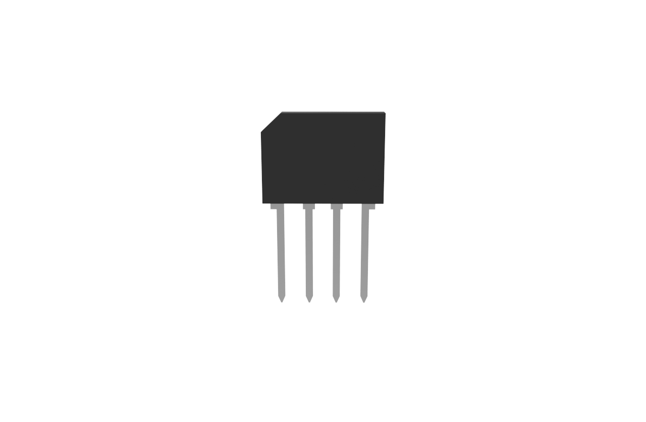 KBP301G-BP datasheet
by Micro Commercial Components
KBP301G-BP datasheet
by Micro Commercial Components