A 4-layer PCB with a solid ground plane and a separate power plane is recommended. Keep the input and output capacitors close to the device, and use short, wide traces for the power lines.
Ensure that the output capacitor has a low ESR, and the input capacitor has a high capacitance. Also, add a small ceramic capacitor (e.g., 10nF) between the VIN and GND pins to filter out high-frequency noise.
Although the datasheet specifies a maximum input voltage of 5.5V, it's recommended to limit the input voltage to 5V to ensure reliable operation and prevent damage to the device.
The output voltage ripple can be estimated using the formula: ΔVout = (Iout * ESL) / (Cout * fsw), where ESL is the equivalent series inductance of the output capacitor, Cout is the output capacitance, and fsw is the switching frequency.
A 10uF to 22uF ceramic capacitor (X5R or X7R dielectric) is recommended for the input capacitor. This value provides a good balance between input ripple rejection and stability.
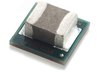 LMZ10500SILT datasheet
by Texas Instruments
LMZ10500SILT datasheet
by Texas Instruments
 Findchips
