-
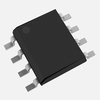
The maximum power dissipation of the LT1011AIS8 is dependent on the package and thermal environment. For the SO-8 package, the maximum power dissipation is approximately 1.3W at 25°C ambient temperature, with a thermal resistance (θJA) of 90°C/W.
-
To minimize noise and ensure stability, it's essential to follow good PCB layout practices, such as keeping the input and output traces separate, using a solid ground plane, and placing decoupling capacitors close to the op-amp. Additionally, avoid routing high-frequency signals near the op-amp's inputs and outputs.
-
While the LT1011AIS8 is an op-amp, it can be used as a comparator in some applications. However, it's essential to note that the op-amp's output stage is not designed for high-speed switching, and the device may not provide the same level of performance as a dedicated comparator. Additionally, the op-amp's input common-mode range and output swing may not be suitable for all comparator applications.
-
The recommended decoupling capacitor value for the LT1011AIS8 is typically in the range of 0.01μF to 0.1μF, with a voltage rating that matches or exceeds the op-amp's supply voltage. A ceramic capacitor with a low equivalent series resistance (ESR) is recommended.
-
The LT1011AIS8 is specified to operate over a temperature range of -40°C to 125°C. However, the device's performance may degrade at higher temperatures, and the maximum junction temperature should not exceed 150°C. For high-temperature applications, it's essential to ensure that the device is properly heatsinked and that the thermal design is adequate.
 LT1011AIS8 datasheet
by Linear Technology