-
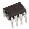
The maximum power dissipation of the LT1013IN8 is dependent on the package and thermal environment. For the 8-pin PDIP package, the maximum power dissipation is approximately 1.3W at 25°C. However, this can be derated to 0.65W at 70°C. It's essential to consult the datasheet and perform thermal calculations to ensure the device operates within safe limits.
-
To minimize noise and ensure optimal performance, it's crucial to follow good PCB layout practices. Keep the input and output traces short and separate, use a solid ground plane, and avoid running high-frequency signals near the op-amp. Additionally, decouple the power supplies with capacitors and use a low-ESR capacitor for the bypass capacitor. Consult the datasheet and application notes for more detailed guidance.
-
The recommended capacitor value for the bypass pin (Pin 8) is 0.01μF to 0.1μF. A 0.1μF capacitor is a good starting point, but the optimal value may vary depending on the specific application and noise environment. It's essential to ensure the capacitor is a low-ESR type and is placed close to the bypass pin.
-
Yes, the LT1013IN8 can be used as a unity-gain buffer. However, it's essential to ensure the output is properly terminated to prevent oscillations. A 1kΩ to 2kΩ resistor in series with the output can help stabilize the circuit. Additionally, the input impedance should be matched to the source impedance to prevent signal attenuation.
-
The LT1013IN8 has internal ESD protection, but it's still essential to handle the device with care. Use an anti-static wrist strap or mat, and ensure the workspace is ESD-safe. Avoid touching the pins or handling the device in a way that could generate static electricity. When storing the device, use an anti-static bag or tube to prevent damage.
 LT1013IN8 datasheet
by Linear Technology