-
The maximum power dissipation of the LT1498CS8 is dependent on the package and thermal environment. For the SO-8 package, the maximum power dissipation is approximately 1.4W at 25°C ambient temperature, with a thermal resistance (θJA) of 85°C/W.
-
To minimize noise and ensure optimal performance, it is recommended to follow good PCB layout practices, such as separating analog and digital grounds, using a solid ground plane, and keeping sensitive analog signals away from noisy digital signals. Additionally, the LT1498CS8 should be placed close to the input bypass capacitors and the output filter components.
-
The recommended input capacitance for the LT1498CS8 is 1-10uF, with a low ESR (Equivalent Series Resistance) to ensure stability and minimize noise. The recommended output capacitance is 10-100uF, with a low ESR to ensure stability and minimize output ripple.
-
To protect the LT1498CS8 from overvoltage and overcurrent conditions, it is recommended to use a voltage clamp or a transient voltage suppressor (TVS) at the input, and a current limit resistor or a fuse at the output. Additionally, the LT1498CS8 has built-in overcurrent protection, which will limit the output current to approximately 1.5A.
-
The typical startup time of the LT1498CS8 is approximately 100-200ms, depending on the input voltage and output load. This is the time it takes for the regulator to reach its nominal output voltage after power-on.
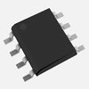
 LT1498CS8 datasheet
by Linear Technology
Findchips
