-
A good PCB layout for the LT6000CDCB#TRMPBF involves keeping the input and output capacitors close to the device, using a solid ground plane, and minimizing trace lengths and widths to reduce parasitic inductance and capacitance.
-
To ensure stability, make sure to follow the recommended component values and PCB layout guidelines, and consider adding a compensation capacitor (CC) to the output stage if necessary. Also, ensure that the input and output capacitors are of high quality and suitable for the operating frequency.
-
The LT6000CDCB#TRMPBF can handle input voltages up to 36V, but it's recommended to operate within the specified input voltage range (2.2V to 36V) for optimal performance and reliability.
-
Choose an output capacitor with a low equivalent series resistance (ESR) and a high ripple current rating. The capacitor value should be selected based on the output voltage and current requirements, as well as the desired output ripple and noise performance.
-
The thermal derating curve for the LT6000CDCB#TRMPBF is typically provided in the datasheet or can be obtained from the manufacturer. It's essential to follow the derating curve to ensure the device operates within its safe operating area and to prevent overheating.
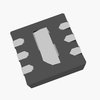
 LT6000CDCB#TRMPBF datasheet
by Linear Technology