To minimize noise and ensure optimal performance, it is recommended to follow a star-grounding scheme, keep analog and digital grounds separate, and use a solid ground plane. Additionally, keep the analog input traces short and away from digital traces, and use a low-ESR capacitor for the AVDD pin.
To optimize the MAX1193ETI+T's analog-to-digital conversion speed and accuracy, ensure that the analog input signal is properly filtered and amplified, and that the reference voltage is stable and accurate. Additionally, adjust the clock frequency and conversion mode to suit the specific application requirements.
To ensure reliable operation over temperature, ensure that the MAX1193ETI+T is properly heat-sinked, and that the PCB is designed to dissipate heat efficiently. Additionally, follow the recommended operating temperature range and avoid exceeding the maximum junction temperature.
To interface the MAX1193ETI+T with a microcontroller or FPGA, ensure that the digital interface is properly configured, and that the clock and data signals are properly synchronized. Additionally, consider the digital interface protocol, data transfer rate, and error detection and correction mechanisms.
To ensure ESD protection, follow proper handling and storage procedures, and use ESD-protective packaging and materials. Additionally, design the PCB with ESD protection in mind, using components such as TVS diodes and resistors to protect the MAX1193ETI+T from electrostatic discharge.
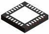 MAX1193ETI+T datasheet
by Maxim Integrated Products
MAX1193ETI+T datasheet
by Maxim Integrated Products
 Findchips
 Findchips