-
A good PCB layout for the MAX5033BASA+ involves keeping the input and output traces separate, using a solid ground plane, and placing the input and output capacitors close to the device. Additionally, it's recommended to use a low-ESR capacitor for the output capacitor to minimize ringing.
-
To ensure stability, make sure to follow the recommended component values and PCB layout guidelines. Additionally, ensure that the output capacitor is properly sized and has a low ESR. If oscillations occur, try adding a small capacitor (e.g., 10nF) between the output and ground to dampen the oscillations.
-
The MAX5033BASA+ can handle input voltages up to 30V, but it's recommended to keep the input voltage below 24V for optimal performance and to prevent overheating.
-
The MAX5033BASA+ is rated for operation up to 125°C, but its performance may degrade at high temperatures. Ensure proper heat sinking and thermal management to prevent overheating and ensure reliable operation.
-
The output voltage of the MAX5033BASA+ can be calculated using the formula: Vout = (R1/R2) * (Vin - Vref), where R1 and R2 are the feedback resistors, Vin is the input voltage, and Vref is the internal reference voltage (typically 2.5V).
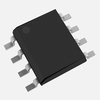
 MAX5033BASA+ datasheet
by Maxim Integrated Products
