-
The recommended power-up sequence is to apply VCC first, followed by VREF, and then the digital signals (SCLK, SDIN, and SYNC). This ensures proper initialization and prevents damage to the device.
-
The analog output filter should be designed to have a cutoff frequency of around 100 kHz to 200 kHz to remove high-frequency noise and ensure a smooth output signal. A simple RC filter or a more complex active filter can be used, depending on the specific application requirements.
-
The maximum allowed capacitance on the VREF pin is 10 nF. Exceeding this value can cause instability and affect the performance of the device.
-
Yes, the PCM1702U-J can be used with a different voltage reference, but it must be within the specified range of 2.5 V to 5.5 V. The voltage reference should also be stable and have low noise to ensure accurate conversion.
-
Clock jitter and skew can be minimized by using a high-quality clock source, such as a crystal oscillator, and ensuring that the clock signal is properly terminated and routed. Additionally, the PCM1702U-J has a built-in clock jitter attenuator that can help reduce the effects of clock jitter.
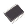
 PCM1702U-J datasheet
by Texas Instruments
 PCM1702U-J datasheet
by Texas Instruments