-
The recommended power-on sequence is to first apply the voltage to the VDD pin, followed by the voltage to the VDDA pin. This ensures that the internal regulators are properly powered up and stabilized before the device becomes operational.
-
The clock tree should be configured to use the highest frequency clock source available (e.g. HSE or PLL) and to enable the clock gating feature to reduce power consumption. Additionally, the clock prescalers should be set to the optimal values for the specific application.
-
The maximum allowed voltage on the GPIO pins is 3.6V, which is the absolute maximum rating. However, it is recommended to keep the voltage below 3.3V to ensure reliable operation and to prevent damage to the device.
-
A reliable reset circuit can be implemented using an external reset IC (e.g. STM811) or by using a simple RC circuit with a capacitor and a resistor. The reset signal should be connected to the NRST pin and should be able to hold the device in reset for at least 10ms.
-
The power supply pins (VDD and VDDA) should be connected to a solid power plane with a low impedance path to the power source. The decoupling capacitors should be placed as close as possible to the power pins and should have a low ESL and ESR. The power supply lines should be routed away from sensitive analog signals to prevent noise coupling.
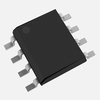
 STM805LM6F datasheet
by STMicroelectronics
 STM805LM6F datasheet
by STMicroelectronics