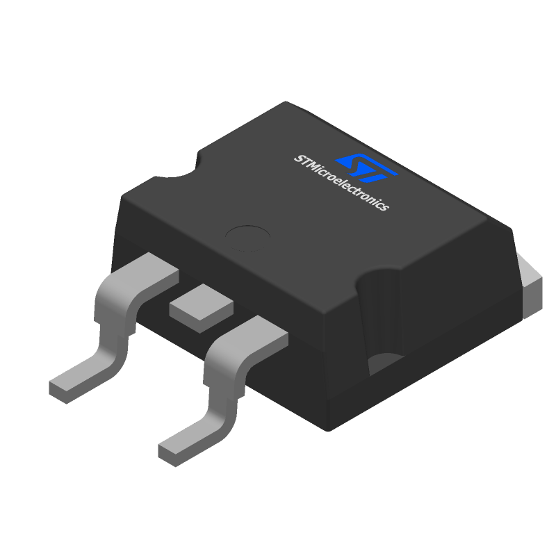
-
A good PCB layout for optimal thermal performance would be to have a large copper area connected to the tab of the device, and to use thermal vias to dissipate heat to the other layers of the PCB.
-
To ensure proper soldering, use a soldering iron with a temperature of 250°C to 260°C, and apply a small amount of solder paste to the pads. Use a soldering technique that minimizes the time the iron is in contact with the device.
-
The maximum allowed voltage on the gate pin is 20V, as specified in the datasheet. Exceeding this voltage may damage the device.
-
To protect the device from ESD, handle the device by the body or use an anti-static wrist strap, and store the device in an anti-static bag or container. Ensure the PCB and assembly process also follow ESD-safe practices.
-
The recommended gate resistor value depends on the specific application and switching frequency. A typical value is in the range of 10Ω to 100Ω, but it's recommended to consult the application note or a qualified engineer for a specific design.
 STPS20H100CGY-TR datasheet
by STMicroelectronics
