-
A 2-layer or 4-layer PCB with a solid ground plane and thermal vias under the device is recommended for optimal thermal performance. The PCB should also have a large copper area connected to the thermal pad to dissipate heat efficiently.
-
To ensure reliable operation at high temperatures, it is essential to follow the recommended thermal design guidelines, use a suitable thermal interface material, and ensure good airflow around the device. Additionally, the device should be operated within the specified junction temperature range (TJ) of -40°C to 150°C.
-
The recommended input capacitor value is 10uF to 22uF, and the type should be a low-ESR ceramic capacitor (X5R or X7R dielectric) to ensure stable operation and minimize voltage ripple.
-
The output voltage ripple can be calculated using the formula: ΔVout = (Iout * ESL) / (Cout * fsw), where ESL is the equivalent series inductance of the output capacitor, Cout is the output capacitance, and fsw is the switching frequency. The output voltage ripple should be minimized to ensure reliable operation.
-
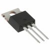
The recommended PCB footprint and land pattern for the STPSC1006D can be found in the STMicroelectronics datasheet or application notes. It is essential to follow the recommended footprint and land pattern to ensure reliable assembly and operation.
 STPSC1006D datasheet
by STMicroelectronics
Findchips
 STPSC1006D datasheet
by STMicroelectronics
 Findchips