-
A good PCB layout for the TDA7233D013TR involves keeping the input and output stages separate, using a star-ground configuration, and placing the device close to the power supply decoupling capacitors. Additionally, using a ground plane and shielding can help reduce EMI.
-
To ensure the TDA7233D013TR operates within its SOA, calculate the device's power dissipation using the formula Pd = (Vin - Vout) x Iout. Then, ensure the device's junction temperature (Tj) remains below the maximum rating of 150°C by providing adequate heat sinking and airflow.
-
When selecting input and output capacitors for the TDA7233D013TR, consider the capacitor's equivalent series resistance (ESR), capacitance value, and voltage rating. A low-ESR capacitor with a high capacitance value (e.g., 10uF to 22uF) and a voltage rating above the input voltage is recommended.
-
To troubleshoot issues with the TDA7233D013TR, start by verifying the input voltage, output voltage, and current. Check for proper PCB layout, decoupling, and component selection. Use an oscilloscope to observe the output voltage and current waveforms, and consult the datasheet and application notes for guidance.
-
The TDA7233D013TR's quiescent current (Iq) contributes to the overall system power consumption, especially in low-power or battery-powered applications. To minimize power consumption, consider using a low-Iq mode or a power-saving feature, if available, and optimize the system's power management strategy.
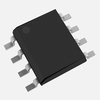
 TDA7233D013TR datasheet
by STMicroelectronics