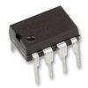
-
STMicroelectronics provides a recommended PCB layout in the application note AN5323, which includes guidelines for component placement, routing, and thermal management to ensure optimal performance and minimize noise.
-
The TS512AIN has a thermal pad that must be connected to a thermal ground plane on the PCB to dissipate heat. A thermal interface material (TIM) can be used to improve heat transfer. The application note AN5323 provides more details on thermal management.
-
The TS512AIN is rated for operation from -40°C to 125°C, but the maximum junction temperature (TJ) should not exceed 150°C. The device should be derated for operation above 85°C to ensure reliability.
-
The TS512AIN has a gain select pin (GAIN_SEL) that can be connected to VCC, GND, or left floating to select one of three gain settings. The gain settings are described in the datasheet, and the application note AN5323 provides more details on gain configuration.
-
The recommended input impedance for the TS512AIN is 50 ohms, which is the standard impedance for most RF and microwave applications. However, the input impedance can be adjusted using external components to match the specific requirements of the application.
 TS512AIN datasheet
by STMicroelectronics