The recommended PCB footprint for the VS-HFA16PA60CPBF is a rectangular pad with a minimum size of 1.5 mm x 2.5 mm, with a 0.5 mm radius corner and a 0.3 mm solder mask clearance.
To ensure reliable soldering, use a soldering iron with a temperature range of 250°C to 260°C, and apply a solder flux with a moderate activity level. Avoid using excessive solder or flux, and ensure the component is properly aligned on the PCB.
The maximum allowed voltage derating for the VS-HFA16PA60CPBF is 10% of the rated voltage, which is 60 V. Therefore, the maximum allowed voltage derating is 6 V.
Yes, the VS-HFA16PA60CPBF is suitable for high-frequency applications up to 1 MHz. However, it's essential to consider the component's parasitic inductance and capacitance when designing the circuit.
Store the VS-HFA16PA60CPBF in a dry, cool place, away from direct sunlight and moisture. Avoid bending, flexing, or applying excessive mechanical stress to the component during shipping and handling.
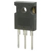 VS-HFA16PA60CPBF datasheet
by Vishay Semiconductors
VS-HFA16PA60CPBF datasheet
by Vishay Semiconductors